Lechler’s Website:
Electronic Equations 3: Content :
- The Basics of quadrupole parameters .
- Series connection of quadrupole’s
- Electronic Tubes basic’s
- Barkhausens Tube Formulas
- Analyse vacuum tube circuits with CAD Programs.
- How to analyse unknown Transistors with CAD programs
- Read bidirectional transistor h parameters from the data-sheet.
- Transistor h parameter equations.
- Transistor y parameter.
- Comparison of vacuum tubes with transistors
- Neutralization of transistors using y parameters.
- Formulas for transistor resonant amplifiers with y parameters
- Transistor S- Parameter equations
- Phase and runtime distortion.
- Delay Equalizer basics.
- Lumped circuits of runtime Equalizers
- Step by step development of run time equalizers.
The Basics of quadrupole parameters for electronic components
Analog electronics units and components can be considered as a black boxes of whose contents we do not know. They are defined by their input and output data. This black boxes are called n-Port . At Fig.1,2,3 we see a 2 port to explain the parameters. The definition can be done with the following 4 parameters which are of course complex values:
- Fig.1 , H-parameters are use full in the kHz Range.
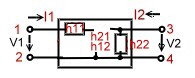 :
: - V1= H11 I2 + H12 V2 ; I2 = H21 I1 + H22 V2 ,
- H11= [V1/I1] !V2 =0 ; H22 =[I2/V2] !I1=0
- H12 =[V1/V2] !I1=0 ; H21 =[I2/I1] !V2=0
- Fig.2 , Y -parameters are use full in the MHz range.:

- I1 = Y11 V1 + Y12 V2 ; I2 = Y21 V1 + Y22 V1 ;
- Y11 =[I1/V1] !V2=0; Y22 =[I2/V2] !V1=0;
- Y12 =[I1/V2] !V1=0; Y21 =[I2/V1] !V2=0;
- Fig.3 , Z- Parameters are use full in Filters.
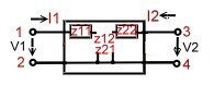
- V1 = Z11 I1 + Z12 I2 ; V2 = Z11 I1+ Z22 I2 ;
- Z11 =[V1/I1] !I2 =0 ; Z22 = [V2/I2] !I1 =0 ;
- Z12 =[V1/I2] !I1 =0 ; Z21 =[V2/I1] ! I2 =0 ;
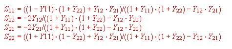
- S-Parameters (Scattering Parameter)are use full in the MHz and GHz range.
- >>> Link to S parameter definition
The complex Quadrupole parameters at the same frequency, can be converted into one another:
- H11 = dZ/Z22 ; H12 = Z12/Z22 ; H21 = - (Z21/Z22) ; H22 = 1/Z22 ;
- H11 = 1/Y11 ; H12 = - (Y12/Y11) ; H21 = Y21/Y11 ; H22 = dY /Y11;
- Y11 = Z22/dZ ; Y12 = -(Z12/dZ) ; Y21 = - (Z21/dZ); Y22 = Z11/dZ ;
- Y11 = 1/H11 ; Y12 = -(H12/H11); Y21 = H21/H11 ; Y22 = dH/H11;
- Z11 = dH / H22 ; Z12 = H12 / H22 ; Z21 = -(H12 / H22 ); Z22 = 1 / H22 ;
- dZ = Z111Z22 - Z12Z21 ;
- dH = H11H22 - H12H21 ;
- dY = Y11Y22 - Y12Y21;
- Change from Y to S parameter
 |
Series connection of Quadrupoles
Two quadrupoles in series. Fig.1 can be computed, to be one quadrupole, if the H or S parameter of the block are known. Y-parametres must first changed into H or S parameters and vice versa:.
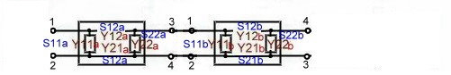 |
- Series formula for H.parameters:
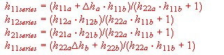
- Series formula for S.parameters :
Electronic Tubes basic’s, understanding, application, formulas.
There are still many friends of electronic vacuum tubes. The behaviour of vacuum tubes in a circuit can be calculated with the formulas of Barkhausen, but can not be analysed with modern CAD programs, because these programs do not have data blocks of tubes installed. There are mainly 4 kind of tubes used , which have different curves. Fig.1(without filament):
- -Diode, -Triode, -Pentode, -Pentode with brake grid.
Fig.1 Electronic-tubes and their curves
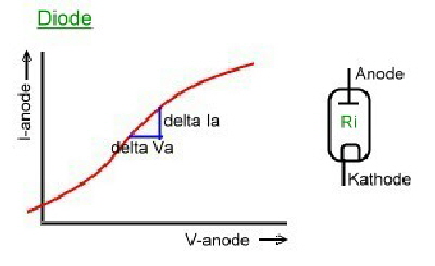
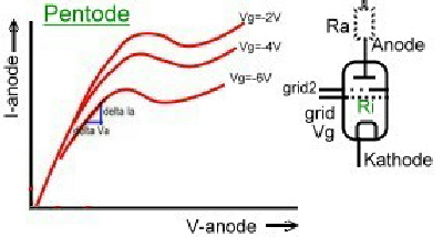
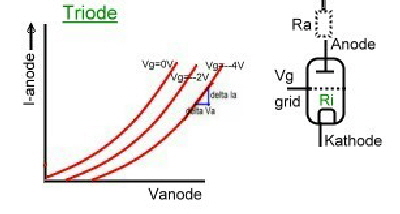
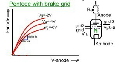
Electronic tubes have a very high-ohm input grid and its output resistance is in the kOhm range. The tube general formulas without parasitic's , are:
- Slope = dJa/dVa.
- Reaction D=1/u.
- Unloated Gain u=dVa/dVg.
- Inside resistance Ri=dVa/dIa
- S D Ri=1
- Gain = Va(~) /Vg(~)
- Va(~) = -S Vg(~)(RiRa)/(Ri+Ra)
How to analyse vacuum tubes using CAD Programs
Here is a very simple way to analyse tubes with an analysis program, if the program has an Y parameter quadrupole block.(n-port ). The things we need are the y parameters versus frequency of the tube, which must be written in a CAD-Y 2 Port Block. The Y parameters of vacuum tubes are :
- Ygk = (Grid / Cathode) Admittance
- Yag = (Anode / Grid) Admittance
- Yak = (Anode / Cathode) Admittance
- S = Slope = (delta Ja/ delta Ug) = (Gain)
This Values can be computed from Capacitance’s and Resisters found in tube Catalogues. Catalogue values are resistor and capacitor values >>>Y = 1/ R . To analyse in a CAD program, we nee values over the frequency working range.
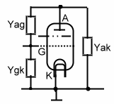 Fig.1 Tube Data
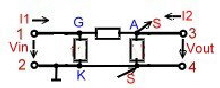 |
Fig.1 Tube 2 Port
- Yag = (omega)*Cga;
- Ygk = (omega)*Ce + (1/Rg+1/Ri));
- Yag = (omega)*Ca + 1/Ra;
Typical Value are:
- Cga = 0,1pF; Ce =4,6pF; Ca = 6 pF ;
- Rg = 1 MOhm; Ri = 200kOhm; Ra = 200kOhm;
In the following formulas, the regular quadrupole formulas are enhanced due of the gain slope S.
Y11, Y22, Y12 , Y 22 are values to be written in a CAD Y- Block like Fig.2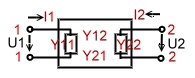 Fig.2 Y- Block
Y parameter of tubes in Cathode common circuits
- Y11 = Ygk + Yag
- Y12 = -Yag .
- Y21 = S -Yag .
- Y22 = yak + Yag.
To analyze a circuit without a Cad Block we can use :
- Y22x = Yak +Yag + Yag((S-Yag)/(Ygk + Yag)).
- Y11x = Ygk +Yag .+ Yag((S-Yag)/(Yak + Yag)).
- Gain = V2/V1 = -(S-Ag) /(Yak + Yag) >>> Load must be part of Yak.
Y parameter of tubes in Grid common circuits
- Y11 = S + Yak + Ykg;
- Y12 = -Yak,
- Y21 = -(S + Yak );
- y22 = Yak + Yag;
To analyze a circuit without a Cad Block we can use :
- Y11x = S + Yak +Yag -Yak((S +.Yak) / (Yak + Yag)).
- Y22x = Yak +Yag - Yak((S + Yak) / (S + Ykg + Yak)).
- Gain = V2/V1 = (S + Yak) / ( Yak + Yag); >>> Load must be part of Yag.
Y parameter of tubes in Anode common circuits
- Y11 = Ykg + Yga
- Y12 = -Ykg
- Y21 = -(S -Ykg).
- Y 22 = S + Ykg + Yka;
To analyse a circuit without a Cad Block we can use :
- Y11x = Ygk +Yga - Ykg((S + Ykg) / (S +Ykg + Yka));
- Y22x = S + Ykg +Yka - Ykg ((S +Ygk) / (Yga +Ykg);
- Gain = V2/V1 = ( S + Ygk) / (S + Ygk + Yka), >>> Load must be part of Yka.
------------------------------------------------------------------------------------------------------------------Analysing the tube with CAD
The Y values Y11, Y22 , Y12, Y21, depending on the frequency, must be written in a CAD Y Block, for instance as a touchstone format . The blue text must be written as a ASC2 DOS text-file.
- ! filename.Y2P
- ! filename
- # HZ S MA R 50 Z
- ! Y-PARAMETER DATA
- 1.200E+08 9.558E-01 -1.486E+02 2.632E-02 5.941E+01 2.632E -02 5.941E+01 9.544E-01 1.062E+02
- NEXT FREQUENCY AND DATA .......AND SO ON
frequency Y11 Y11angle Y21 Y21angle Y12 Y12angle Y22 Y22angle
OR FIRST COMPUTE THE Y PARAMETERS INT0 S-PARAMETRS AND ANALYSE THE S -PARAMETER-BLOCK USING ‘APPCAD’
How to analyse unknown Transistors with CAD programs
If we want to analyze circuits with transistors, whose data’s are not available in the program , You can write the Data’s of the transistor in a 2-Port Block. But one must know, the quadrupole data’s of the transistor.We write the transistor 2 Port values in a standard S , Y or H block. This are values from catalogue , where sometimes other names are used. Static H Parameters can be read directly from the Data sheet..
Read bidirectional transistor h parameters directly from the datas-heet.
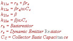
When the transistor cross frequency is ten times higher than the operating frequency, one can use static H parameters for circuit analysis. H Parameters can be read directly from the Data sheet.. Fig. We find these data from the slope of the curve at the working point.
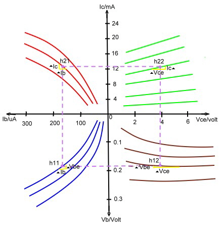 Fig. H parameter emitter common circuit in the data sheet.
The h-parameter are defined as :
Transistor H parameter equations.
To compute the behavior of a circuit with h parameters, we use the 2 Port of Fig1.
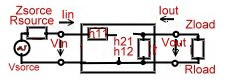 Fig.1 Loaded H- parameter 2 port.
Knowing the H- parameters of a transistors, we have a lot of formulas for design. First, we should know that H parameters are complex values having a real part and a imaginary part. For the emitter common circuit we have the following Formulas:
- Input impedance:
- Voltage Gain :
- Current Gain :
- Output Impedance
- Power Gain

Transistor Y-parameter equations
:Knowing the Y-parameters of a transistor, we have a lot of formulas for design. First, we
should know that Y-parameters sometimes have other names and are complex values having a real part and a imaginary part. For the emitter common circuit we have the following Formulas: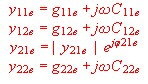
- input admittance (catalogue values)
- feedback admittance (catalogue values)
- Gain admittance (catalogue values)
- Output admittance (catalogue values)
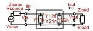
To compute the behavior of a circuit with Y parameter, we use the 2 Port of Fig.
: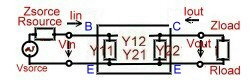 Fig1 Loaded Y-2 Port (Common Emitter)
- Input impedance
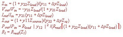
- Voltage Gain
- Current gain:
- Output impedance
- Power gain :
Rsource and Rload are the real parts of Zsorce and Zload.
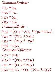
To change from common emitter to basec. or collectorc. circuit, the following formulas are valid:
- Y-Parameter of a Common Emitter circuit:
- Y-Parameter of a Common Base circuit:
- Y-Parameter of a Common Collector circuit:
-
Comparsion of y-parameters of vacuum tubes with transistors
The comparison of a vacuum tube with a transistor is possible if the two-port of the transistor and the 2-port of the tube are equivalent. This requires a transistor 2 - Port with the gain slope S. We obtain the equivalent circuit of Figure 2 with new Y-parameters Y1,Y2,and Y3 :
 New Quadrupole Y- parameters including tubes gain steepness S .
With this new 2 port, we can use tube circuit Formulas in transistor circuits:
This values now can be compared with the tube 2 port: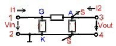
Fig.1 tube 2-port Fig.2 Transistor 2-Port
Neutralization of transistor reaction
The stability of an loaded Transistor amplifier depends on the value of the Collector basis
admittance. This reaction of “bad” transistors can be neutralized using a feedback admittance.Fig.1 
Fig.1 Neutralized transistor 2-port ((Emitter common)
We have the following Formulas with a “new” transistor and new y-parameters:
Fig.2 “New” transistor due of neutralization
 |
- y11n = y11-y12/n;
- y12n = 0;
- y21n = y21-y12/n ,
- y22n = y22 - y12/n ;
Formulas for transistor resonant amplifiers with y parameters
Fig.1 Two stage transistor amplifier
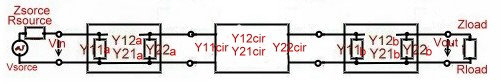 |
To find the gain formulas for a resonator loaded transistor amplifier, we must use the formulas for series connection of quadrupoles. Fig.1 shows the blocks of a resonator loaded 2 transistor amplifier . This would be the work of a computer program. For simple circuits we can use the following gain formulas:
- If the cuircuit between the transistors is a Single Resonator follows:
: 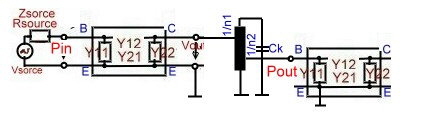
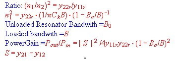
Fig.2 Y parameter and resonator
- If the cicuit betwen the Tansistors is a Two Resonator Butterworth band filter :
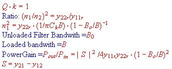
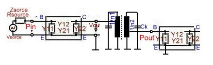 Fig.3 Y parameter and bandpass
Transistor Gain, using S- Parameter equation.
Transistor Amplifier design at higher frequencys, are best realized using the S parameter
Formulas .But even at low frequencies ,S-Parameter(Scattering Parameter) are very helpfull. For the case of matched input of a transistor, the gain is:![]() Transistor S-Values
Transistor S-Values
Electronic signals which carry communication content, go through circuits, filters, long distance cables and communication satellite networks . If the phase response of a signal path is not proportional to frequency response, phase and runtime distortions of the signal, will occur. The consequence is that language twitters and images are blurred.
The runtime of the phase is called tp.
tp = b/(omega).
Electronic communication signals consists of many frequencies therefore his run time is called : “group’s run time = tg” , tg is computed with the following differential equation :
tg = db/d(omega).
Fig.1 shows the example of the phase constant of a circuit and its differential quotient
Only if tg is constant over the working frequency range, there are no distortions. The absolute value of tg is not important. Otherwise, a delay equalizer must be installed in the circuit, or somewhere on the net. .The delay
equalizer should not affect the amplitude of the transfer, but should linearize the phase. Fig.1b shows a typical data bit sent over a communications system:
Courve #1: Data bit in a system without
groups runtime compensation
Courve #2: Databit in an equalizer linearized system
Obviously, the bits in the phase linearized communication system are faster and have less overswing.
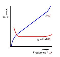 Fig.1 Groups Run Time tg and Phase Constant b versus Frequency
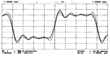 |
Fig.1b Data bit’s in a communication system:
Delay Equalizer basics of RF-communication electronics.
Delay Equalizer are electronic circuits or layouts or microwave wave-guides, which keep the
running time on a constant value, over the bandwidth of a communication system, to avoid distortions. See Fig.1
Regardless of the type of equalizer and their practical implementation, runtime versus
frequency can be realized, in mathematical form using a Hurwitz-polynom and poles, located in a coordinate system as Figure 2 shows. For a stable system, we consider only the
poles in the left side. The location of a pole is defined as :
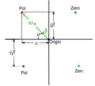
Fig.2 Poles and zeros definition
- Angel of pointer:


The general transmission equation using the Hurwitz Polynom is :
The definitions are:
- s = Normalized frequency:
- p = Unnormlized frequency:
- fn = Polfrequency:
- fb = Frequency of reference:
- Q = Polquality:
- Z = numerator:
- N= denominator:
In the special case of the run-time equalizer, we get :
![]()
The result of the transmission equation F(s) is gain an phase.
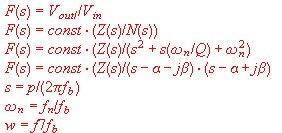
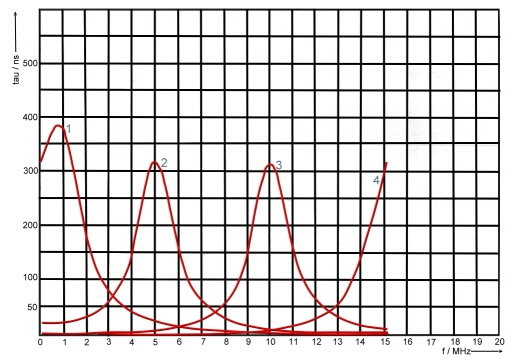
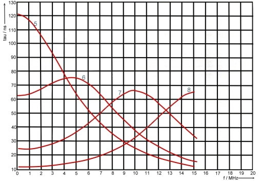
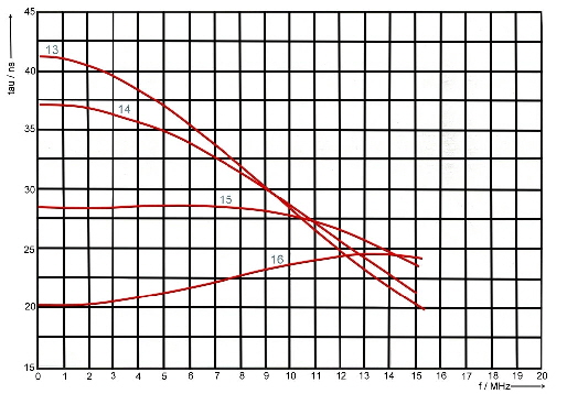
Groups run time is as we have already seen: tg = db/d(omega). With the help of a computer program, we can calculate phase and runtime depending on the frequency. As an example at Fig.3 to 6, gruops runtime depending on alpha and beta is shown in the 10 MHz range .The numbered parameter courves at Fig.3-6 are:
#of courve, Alpha , Beta, Phase
- 1, -0,1, 0,1, 85
- 2, -0,1, 0.5, 84
- 3, -0.1, 1.0, 78
- 4, -0.1, 1.5, 45
- 5, -1, 0.1, 6
- 6, -0.5, 0.5, 4 5
- 7, -0.5, 1.0, 63
- 8, -0.5, 1 .5, 71
- 9, -1, 0.1, 6
- 10, -1, 0.5, 36
- 11, -1, 1.0, 45
- 12, -1, 1.5, 56
- 13, -1.5, 0.1, 4,
- 14, -1.5, 0.5, 18
- 15, -1.5, 1.0, 33
- 16, -1,5, 1.5, 45
:
Fig.3 -6 Groups runtime tau(omega) versus alpha and beta in the 10 MHz range.
 |
 |
 |
 |
Step by step development of groupdelay equalizers.
The following practical way of developing a group’s runtime Equalizer, is helpful and proven:
- Write a computer program in any language, to solve the general groups run time F(s) formula.{1},{2} to find alpha and beta curves versus the considered frequency, similar to fig.3-6
- Find alpha and beta curves with a approximate graphical consideration to get the sum of filter runtime and equalizer runtime constant
- Find an equalizer circuit to realize the necessary alpha and beta values from Fig. 8-12. It is often better to use 2 ore more simple Equalizer in series than only one complex circuit.
- Find the phase = Phs f(omega), which produces the groups runtime of the system.
- Write Phs into a CAD -linear analysing-Program, S-Parameter Block. S21 and S12 > 30dB; S12>30dB ,S21=0db and phase of the system.
- Write the Equalizer circuit into the same CAD-linear analysing-Program.
- Analyse the sum of runtime and the total gain. Runtime must be constant versus frequency.The equalizers gain must be constant versus frequency.
- Add component losses and optimize circuits values during CAD sessions..
.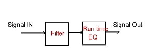 Fig.7 shows as an example the groups run time compensation of a filter
Fig.7 Implementation of a groups run time Equalizer
:
RF circuits equalizer with discrete components, see the following chapter:
Lumped circuits of runtime Equalizers
There are many circuits for runtime equalizers with discrete components
We differ between 5 circuits to be used for different phase angels determined from alpha and beta :![]()
- Equalizer #1: Grade =2; Beta=0;
- Equalizer #2: Grade =4; 0<phi<90degree.
- Equalizer #3: Grade =4; 60<phi<90degree.
- Equalizer #4: Grade =4; 45<phi<90degree.
- Equalizer #5: Grade =4; 45<phi<60degree.
The circuits and formulas to get basic values are shown in Fig.8-13.This basic basic values
are without dimensions and must be multiplied using Lb and Cb.![]()
Omega(b) is the free choice frequency of reference and will be the runtime peak of the equalizer runtime courve. Rb = Free choice of input and output impedance. For Fig.9, we need a perfect coupled transformer having k=1; At RF frequencies the stray inductance of the transformer should be considered, while analyzing the circuit. Factor m is arbitrary.
Gamma is: ![]()
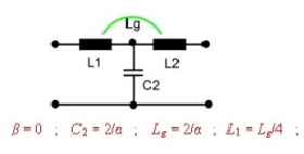 Fig.8 Equalizer #1; 2. order equalizer
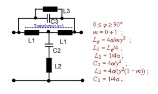 Fig.9 Equalizer #2 ; 4. order equalizer
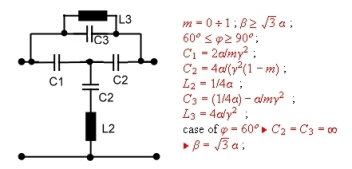 Fig.10 Equalizer #3; 4. order equalizer
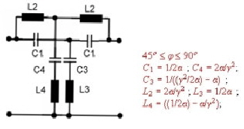 Fig.11 Equalizer #4; 4. order equalizer
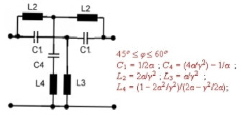 Fig-12 Equaliser #5; 4. order equalizer
Practical Example of groups runtime equalizer .
>>>> Go to groups run time equalizer
Readings for runtime equalizers.
- Microwaves November 1981
- Compact Analysis manual
- Telefunken Zeitung Heft1 1965 Seite 34
- E.Ulbrich, H.Piloty, Über den Entwurf von Allpässen....AEÜ,14, 1960